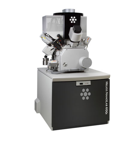
The FEI Helios Nanolab 600 combines emission scanning electron microscope (SEM) with focused ion beam (FIB). It allows the characterization of materials in 2D and 3D (tomography), TEM sample preparation (Lamella), observations at the subsurface of the specimens (cross section imaging) and structural modification of surfaces at the micrometer to nanometer scale. This technique is used in the semiconductor industry, materials science and increasingly in the biological field for site-specific analysis, deposition, and ablation of materials. It is present, in Italy, in few research centres because of its high costs and of the high specialization it requires in the use and interpretation of the results. Nevertheless, because of its potentialities, it is today an indispensable instrument in modern characterisation facilities.